An easier way to design GaN-based power systems: comparing the market’s integrated driver offerings
By Vito Prezioso, Power Specialist Field Applications Engineer, Future Electronics (Northern Europe)

Gallium nitride (GaN) high electron-mobility transistors (HEMTs) offer an exciting new option for power-system designers. Compared to silicon MOSFETs, GaN HEMTs allow them to dramatically reduce switching losses and increase power efficiency, as well as to support higher switching frequencies and so reduce system size and weight.
But the superior performance does not come without a penalty: a GaN HEMT is more difficult to drive than a silicon MOSFET. Whereas a silicon MOSFET needs a simple +10 V drive voltage and can handle transients up to 20 V without the risk of damage, GaN HEMTs can usually accept a maximum gate-drive voltage of just +6 V, and specify an optimal gate-drive voltage of +5 V. Turn-off conditions also have to be carefully managed, some HEMTs require a negative drive voltage to guarantee that the device will not turn on unintentionally. So a GaN HEMT calls for much tighter control of the gate driver’s operation than a silicon MOSFET requires.
This makes an integrated system-in-package (SiP) combining a HEMT and gate driver highly appealing: the HEMT manufacturer can take care of selecting the optimal driver for the HEMT. In the integrated SiP the manufacturer will also implement an optimized gate-drive circuit. The prime benefit of such an optimized circuit is that performance and reliability are not affected by the parasitic inductance to which circuits built with discrete components are prone.
Figure 1 shows where parasitic inductance occurs:
- LS1 is the parasitic inductance due to the gate trace, which connects the Drive pin of the gate driver to the gate of the transistor through a resistor
- LS3 is the inductance generated by the return trace, which connects the Source pin of the transistor to the COM pin of the gate driver
- LS2 is the stray inductance attributable to the source leg, which also affects the power loop
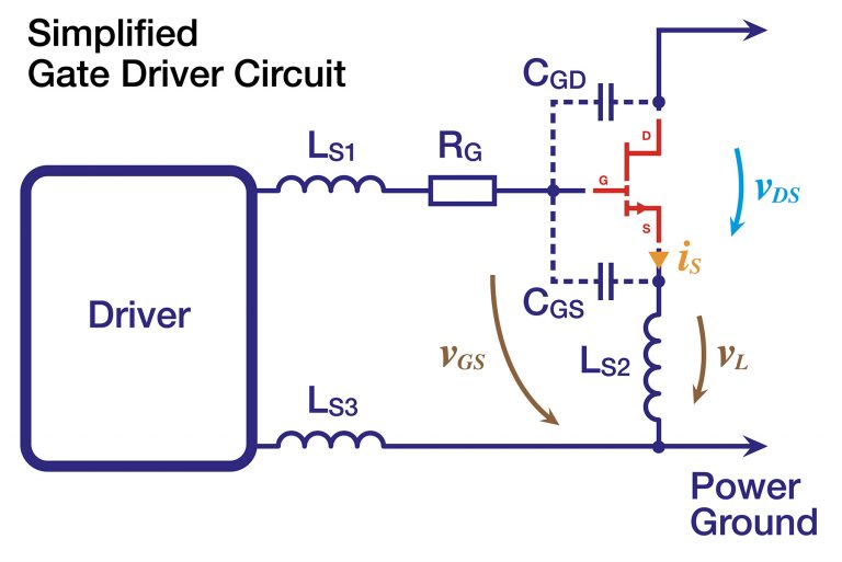
Fig. 1: Simplified gate-driver circuit showing the sources of parasitic inductance
The parasitic inductances, combined with Miller capacitance at a fast-switching transition, can introduce ringing and overshoot or undershoot voltage spikes at the gate. In the best case, this only generates EMI and impairs efficiency; in the worst case, it can actually damage the transistor.
In general, the wider the traces and the shorter the gate drive loop the better. With the driver and transistor combined in a single package, the gate-source loop is kept very short, resulting in substantially lower parasitic inductance than in a circuit with discrete HEMT and driver devices.
The best integrated devices in fact have extremely low stray inductance in the gate-drive loop. This almost eliminates gate-source voltage ringing, with the effect of:
- Lowering stress on the gate structure, and therefore improving the reliability of the HEMT
- Reducing the damping resistance on the driver output. This allows for faster switching and thus lower switching losses.
Integrated devices also offer lower stray inductance in the power loop, greatly reducing drain-source voltage spikes. This results in:
- Lower switching losses
- Lower EMI
- Lower drain-source voltage stress, improving reliability
On top of this, an integrated device offers a reduced component count and board footprint. Some single 650 V, 150 mΩ HEMTs which designers can find on the market today have a footprint of 8 mm x 8 mm. In an application, they require a discrete gate driver and gate-drive resistors. Compare this to the IGI60F1414A1L from Infineon: this CoolGaN™ Integrated Power Stage (IPS) device combines a half-bridge power stage consisting of two 600 V/140 mΩ enhancement-mode GaN switches with dedicated gate drivers in a thermally enhanced 8 mm x 8 mm QFN-28 package.
Different products for different design requirements
These advantages, of easier design implementation, lower parasitic inductance, and smaller board footprint, have led all the main manufacturers of GaN HEMTs to build portfolios of integrated devices alongside their catalogs of discrete HEMTs and GaN drivers.
But certain trade-offs are associated with the use of integrated devices. First is that the customer’s production is more tightly bound to the manufacturer and device: unlike a discrete HEMT and discrete driver, which might in many cases have an industry-standard footprint, an integrated driver device might offer fewer pin- or footprint-compatible alternative sources.
Beyond this, integration also hands to the device manufacturer the decision about how to manage trade-offs and meet the requirements of different types of applications. This means that there are important differences between the integrated GaN products on the market today.
The most striking ways in which the market’s offerings vary are:
- Whether optimized for a specific topology or not
- Whether the device provides a means to adjust operation so as to minimize electro-magnetic emissions at the expense of efficiency
- The additional functions integrated into the device, in addition to the driver and HEMT
Topology-specific integrated GaN products
With the launch of the MasterGaN family, STMicroelectronics took a unique space in the market for integrated GaN products. This is because these GaN SiPs were the first to feature an integrated half-bridge in either a symmetrical or asymmetrical configuration, paired with an optimized 600 V half-bridge driver.
ST created a family of five series of MasterGaN products to address the range of topologies which most customers use, and the range of power ratings which their applications require. So as Figure 2 shows, the MasterGaN2 and MasterGaN3 products are only for use in an active clamp flyback converter, since this topology calls for a lower on-resistance on the low side than on the high side. A new reference design from ST, the EVLONE65W, shows how much space can be saved when combining MasterGaN2 with the ST-ONE all-in-one digital power controller. EVLONE65W is a 65 W USB Power Delivery 3.1 charger board based on an active clamp flyback topology. Measuring 5.8 cm x 3.2 cm x 2.0 cm, the EVLONE65W achieves high power density of 30 W/in³.
For LLC resonant topologies, a symmetrical configuration is provided by the MasterGaN1, MasterGaN4 and MasterGaN5 series, supporting power ratings, according to ST, up to 400 W.

Fig. 2: With the MasterGaN family, ST introduced the industry’s first integrated GaN half-bridge products
In fact, Future Electronics has developed a feature-rich development platform, called GaNSTar, which can supply a maximum load of 500 W using the MasterGaN1. GaNSTar implements a 96%-efficient LLC resonant dc-dc converter. It benefits from a precise digital control scheme running on the board’s STM32G4 microcontroller and exemplary thermal design.
The MasterGaN products are, then, optimized for one of two soft-switching topologies. By contrast, integrated GaN devices from other important suppliers of GaN switches, with onsemi set to release 650 V integrated driver GaN products before the end of 2022, and Infineon with its IGI60F1414A1L CoolGaN IPS device, handle hard switching and are suitable for use in any topology. For instance, evaluation boards in development by onsemi implement converter designs including a 500 W totem-pole power factor correction converter, a 65 W flyback converter, and a 300 W LLC converter.
Managing the EMI vs efficiency trade-off
In another respect, however, the Infineon CoolGaN IPS family is distinct from all the other integrated GaN devices on the market. These Infineon parts allow the power-system designer to access the gate of the transistors, and configure the gate-drive resistors/capacitor to adjust the ratio of dV/dt, as shown in Figure 3. This unique capability enables the designer to manage the balance of switching loss, electromagnetic emissions and overshoot, which can be valuable in applications which have a high sensitivity to EMI. There is a trade-off, however: the addition of the selectable external resistor lengthens the gate-source loop, which, as described above, increases parasitic inductance.
Like onsemi, Infineon has a pipeline of reference board designs based on the CoolGaN IPS family, including a 65 W quasi-resonant flyback converter for a high-density power adapter, and a 65 W active clamp flyback converter.

Fig. 3: An external resistor controls the dV/dt rate in CoolGaN IPS devices
Deeper integration to reduce component count and board footprint
Integration of an optimized driver with its GaN HEMT provides value in part because it reduces development time and effort. This benefit can be extended beyond integration of the driver, however, as Power Integrations demonstrates. True to its name, Power Integrations specializes in the provision of multi-function products. The InnoSwitch™3 and InnoSwitch4 low-power ac-dc converters, for instance, are flyback controllers which integrate PowiGaN™ GaN transistors, a synchronous rectifier controller, and a FluxLink isolated feedback link. These parts minimize the length of the gate-source loop, and enable the designer to realize a very compact and highly efficient design at power levels up to 110 W.
Power Integrations also supplies the HiperPFS-5, a power factor correction controller with integrated 750 V PowiGaN GaN switches.
A useful way to evaluate the Power Integrations approach is with the TobogGaN power-supply board from Future Electronics, shown in Figure 4. This is a 60 W ac-dc converter based on the InnoSwitch3-Pro integrated flyback controller module, which includes a PowiGaN GaN switch on the primary side. Operating from a universal mains input, the TobogGaN system achieves up to 92% efficiency at full load, supplying an output which is programmable between 5 V and 20 V.

Fig. 4: The TobogGaN board from Future Electronics is a flyback converter rated for up to 60 W
Power Integrations does not have this section of the market to itself: it is also worth noting the VIPerGaN products from ST. The VIPerGaN50 is a quasi-resonant flyback controller paired with a GaN power switch. Operating from a mains input, it supports loads up to 50 W. ST also supplies the 65 W-rated VIPerGaN65 and the 100 W VIPerGaN100.
Market responding to stimulus of demand
The diversity in the provision of integrated GaN drivers reflects the manufacturers’ attempts to feel the pulse of the market: with demand for GaN products growing fast from a low base, it is yet to become clear whether, for instance, customers will prioritize efficiency and minimization of parasitic inductance over the freedom to control the dV/dt rate.
What is certain is that the market will continue to grow fast, and that GaN device manufacturers are investing heavily in development and production to meet this demand. Happily, then, customers can look forward to the prospect of a growing choice of products with which to optimize their efficient, high-density GaN-based power-system designs.