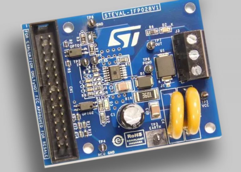
STMicroelectronics

The EVALSTGAP2SICS half-bridge board from STMicroelectronics enables evaluation of the STGAP2SICS, an isolated single-channel gate driver for silicon carbide (SiC) MOSFETs. The STGAP2SiCS produces an output drive current of up to 4 A, and offers galvanic isolation of 6 kV. 

In the EVALSTGAP2SiCS board, the STGAP2SiCS drives a half-bridge power stage with a voltage rating of up to 1,200 V. The components are easy to access on the board and to modify.  

The board supports negative gate driving. Onboard isolated dc-dc converters supply the high- and low-side gate drivers, with maximum isolation of 5.2 kV. 

The configuration of the drive voltage can be easily selected from the following options:

  • +17 V/0 V
  • +17 V/-3 V
  • +19 V/0 V
  • +19 V/-3 V
Rohm

The range of uses for LiDAR sensors is expanding to include not only autonomous driving, but also applications in the industrial and infrastructure fields. Improvements to LiDAR sensors are producing longer range and higher resolution.

In addition to improving the characteristics of the laser diode, it is necessary to drive the laser diode at higher speeds and power. The ROHM RLD90QZWx series is a line of 905 nm, high-power, narrow emission-width laser diodes.

The REFLD002-1 reference design includes the BD2311NVX-LB gate driver to drive the RLD90QZWx laser diode. The high speed of the BD2311NVX-LB contributes to improved LiDAR sensor range and resolution.

Power Integrations

The RDK-877 reference design describes an isolated flyback converter which provides a nominal output voltage of 12 V at 0.5 A load from a wide input-voltage range of 90 V to 305@nbsp;V ac, as well as an isolated zero-crossing detection signal. 

This power supply uses the LNK3306D from the LinkSwitch-TNZ family of ICs. The kit contains the complete power-supply specifications, bill-of-materials, transformer construction, circuit schematic and PCB layout, along with performance data and electrical waveforms.


Power Integrations

The RDK-866 reference design describes a non-isolated buck converter power supply with an input-line zero-crossing detection output signal. The nominal output is 5 V/500 mA across the input range of 90 V to 300 V ac. 

The system is powered by the LinkSwitch-TNZ IC controller. The LinkSwitch-TNZ family of ICs combines power conversion with lossless generation of an ac zero-crossing signal used typically for system clock and timing functions. The device incorporates a 725 V power MOSFET, oscillator, a high-voltage switched current source for self-biasing, frequency jittering, fast (cycle-by-cycle) current limit, hysteretic thermal shutdown, and output and input overvoltage protection circuitry in a monolithic IC. 

Designs using the highly integrated LinkSwitch-TNZ ICs are more flexible than discrete implementations, reducing component count by 40% or more. The key design goal is low cost, low audible noise and compact form factor for use in wireless and relay power supplies.

Monolithic Power Systems

The EVM3804-G-00A provides a ready-made hardware platform for evaluating the MPM3804 step-down switch-mode converter module. 

The module, supplied in a surface-mount 2 mm x 2 mm QFN package, supplies a maximum continuous output current of 0.6 A from an input voltage ranging between 2.3 V and 5.5 V, with excellent load and line regulation. 

The output voltage can be regulated as low as 0.6V. Only input, output capacitors and feedback resistors are needed to complete the design.